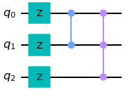
Note that $f(v_1,v_2,v_3)$ can be written as $1\oplus v_1\oplus v_2 \oplus v_3\oplus v_2*v_3 \oplus v_1*v_2*v_3$ where $\oplus$ is the exclusive OR (XOR) and $*$ is AND but written like this is easier to the computation as AND behaves as the usual product and $\oplus$ behaves like a (binary) sum.
You can check it yourself (or using qiskit/python) as shown here
| $v_1$ |
$v_2$ |
$v_3$ |
$f(v_1,v_2,v_3)$ |
output phase |
| 0 |
0 |
0 |
1 |
1 |
| 0 |
0 |
1 |
0 |
-1 |
| 0 |
1 |
0 |
0 |
-1 |
| 0 |
1 |
1 |
0 |
-1 |
| 1 |
0 |
0 |
0 |
-1 |
| 1 |
0 |
1 |
1 |
1 |
| 1 |
1 |
0 |
1 |
1 |
| 1 |
1 |
1 |
0 |
-1 |
Here output phase is the global phase of the circuit output state.
If you can write the function in terms of AND and XOR, then it is straightforward. For this case the $x*y*z$ represents the CCZ gate, the $y*z$ is just a CX gate and the rest are simple Z gates (the 1 is not important because the system is the same up to a global phae), so we can write it analogously as:

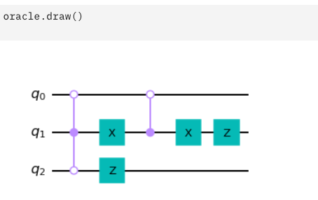
You can also use this rule to read the original circuit, which reads $$v_1v_2v_3\oplus(\neg v_2*v_3)\oplus v_2\oplus v_1$$
$$=v_1v_2v_3\oplus(1\oplus v_2)v_3\oplus v_2\oplus v_1=v_1\oplus v_2 \oplus v_3\oplus v_2v_3 \oplus v_1v_2v_3$$
here I removed the $*$ for easier reading.


